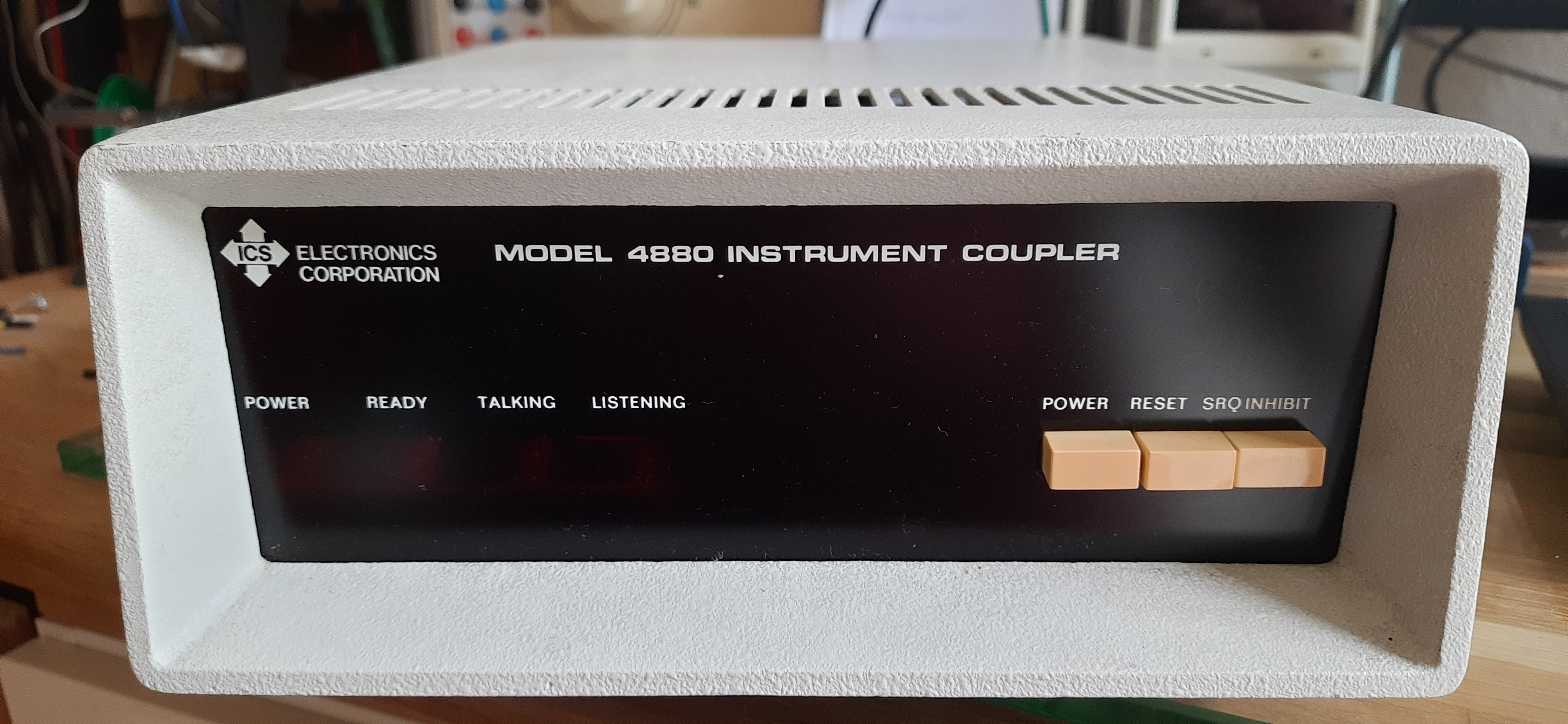
ICS Electronics 4883 Instrument Coupler
This device is from early 1980ies. It’s purpose is to control devices like physical or chemical instruments, not compliant with GPIB, via GPIB bus.
Control happens via digital input and output lines. 4883 has 40 input pins and 40 output pins. Today it can be used as a general digitial IO with 40+40 channels, controllable via GPIB.
There is not much information on this device on the internet.
It looks another company reselled this thing as “PI-952 Pulse Instruments Bidirectional Instrument Coupler”: https://www.artisantg.com/TestMeasurement/61926-1/Pulse-Instruments-PI-952-Bidirectional-Instrument-Coupler
And also it was sold as “Fairchild 4880 Instrument Coupler”.
A hint to manual copy service from ICS from 2017:
“Fairchild Model 4880 Instrument Coupler Instruction Manual”, Rev. 5, 1981, Fairchild Instruments, Los Angeles, CA. (Available for $25 from ICS Electronics, 1620 Banker Rd., Sandose, CA. 95112, Part No. 120002.) Google Scholar”
Details
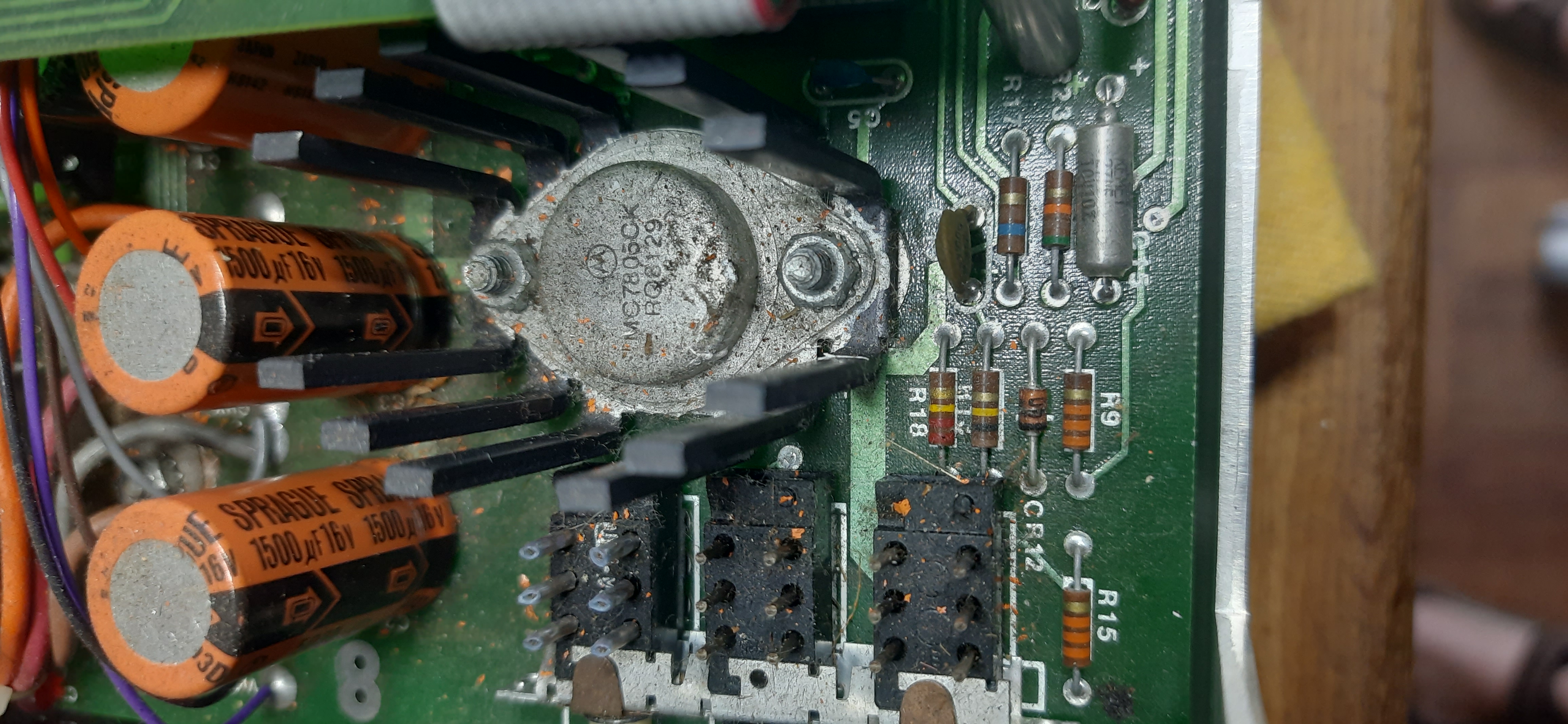
PSU:
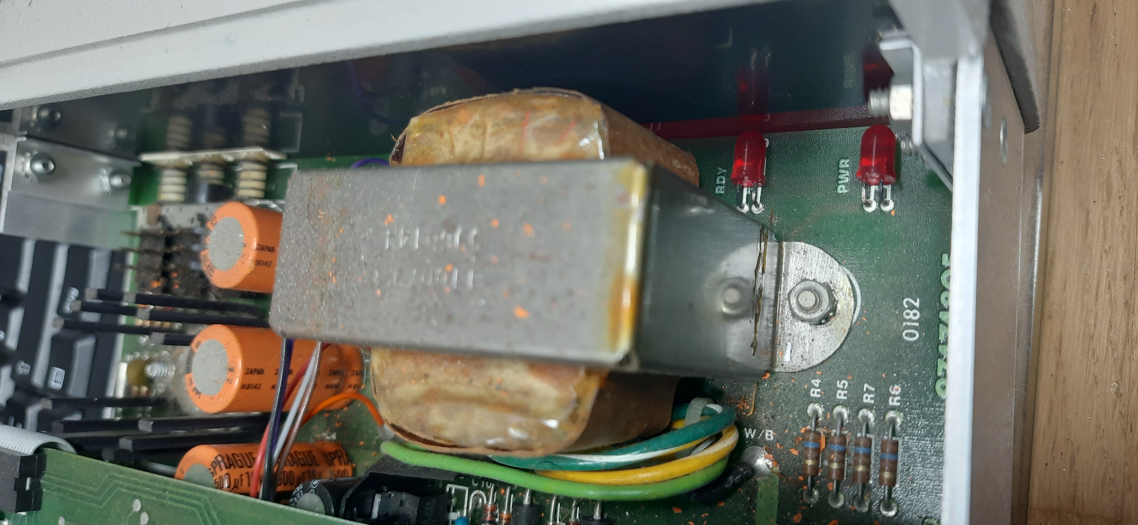
Dirt here and there:
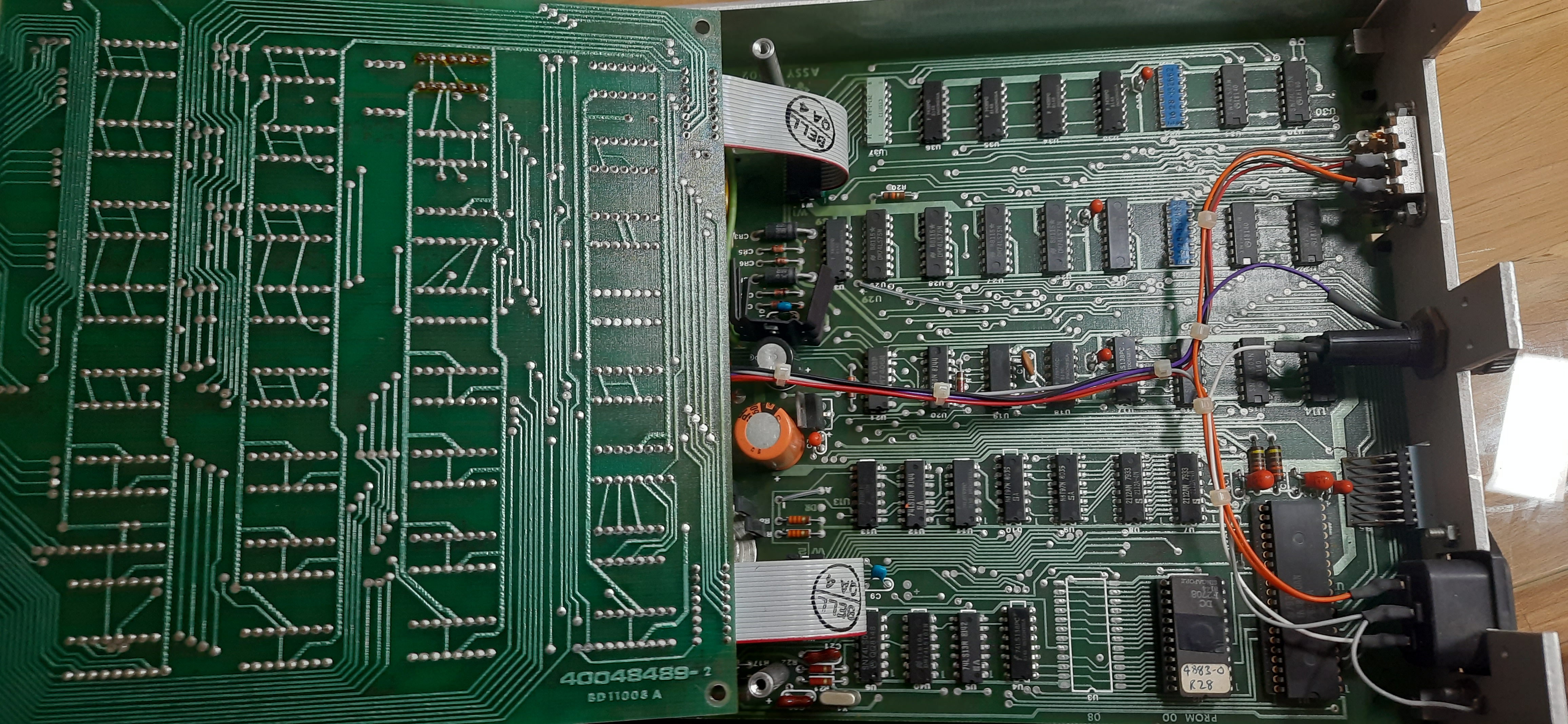
Main board:
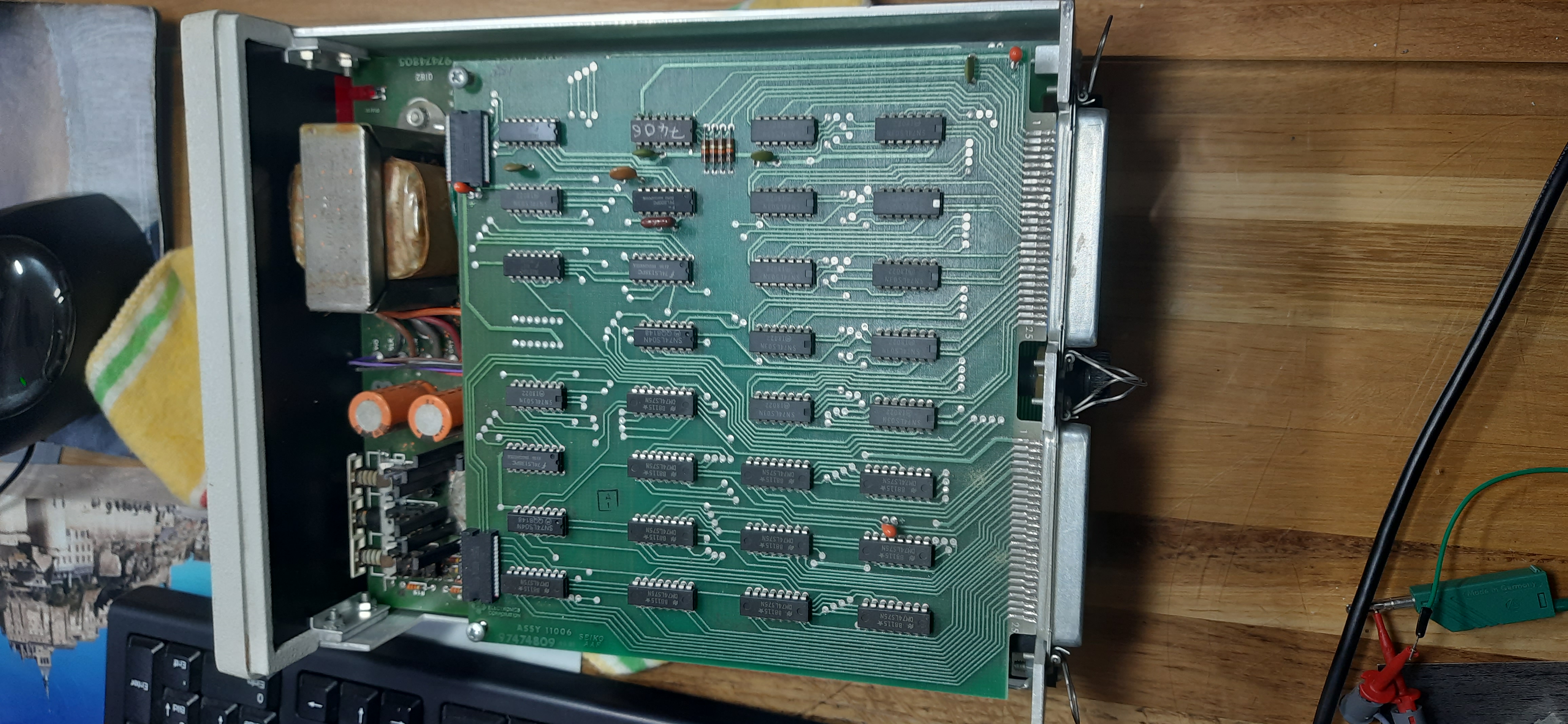
Input/Output board:
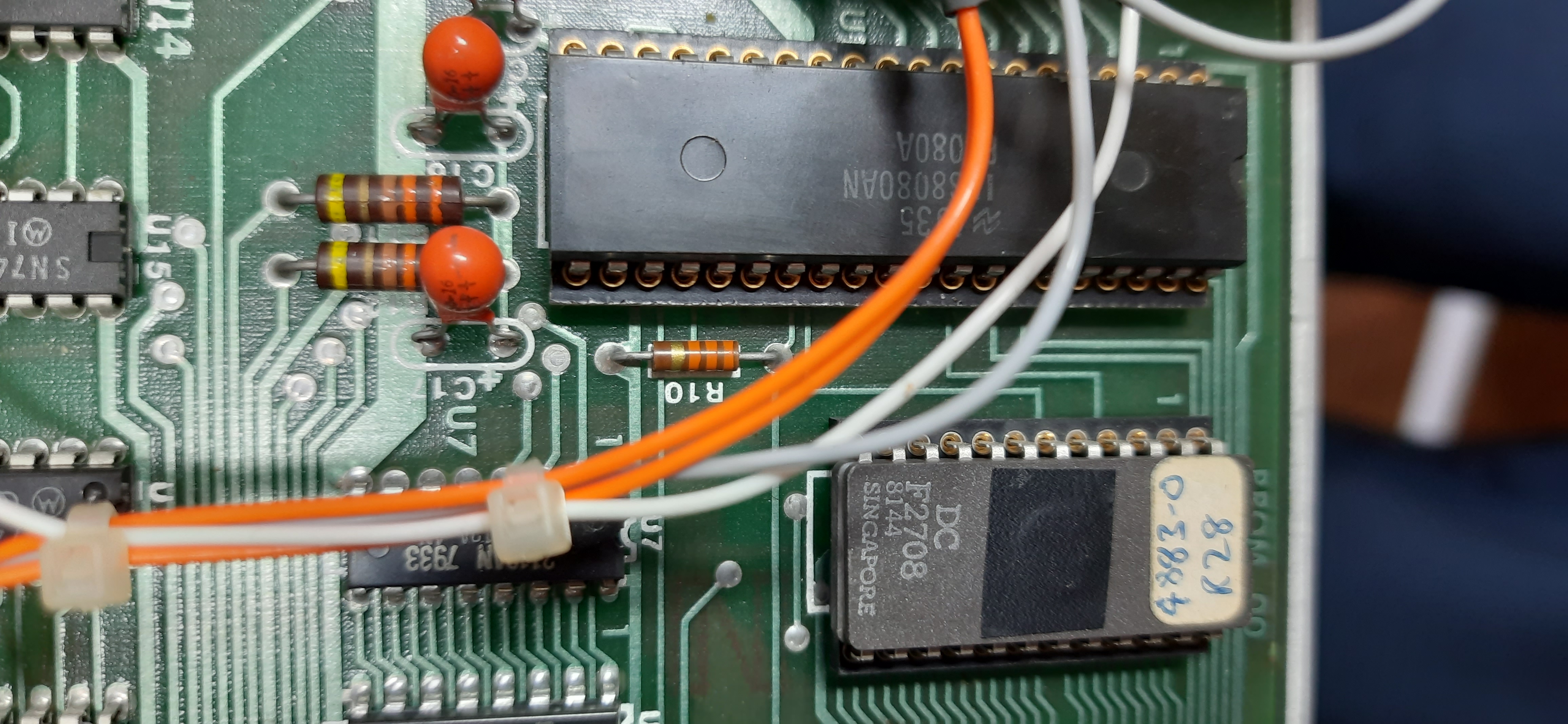
8080 CPU (National Semiconductor INS8080AN P8080A) and 2708 EPROM 1Kx8. There is also some RAM 2x 2112 (256x4, i.e. 1KBit) on board. We have two, so 256x8 Bit, = 258 Bytes RAM. The CPU can run with 2 MHz. Quarz visible has 14.74 MHz.
ROM content
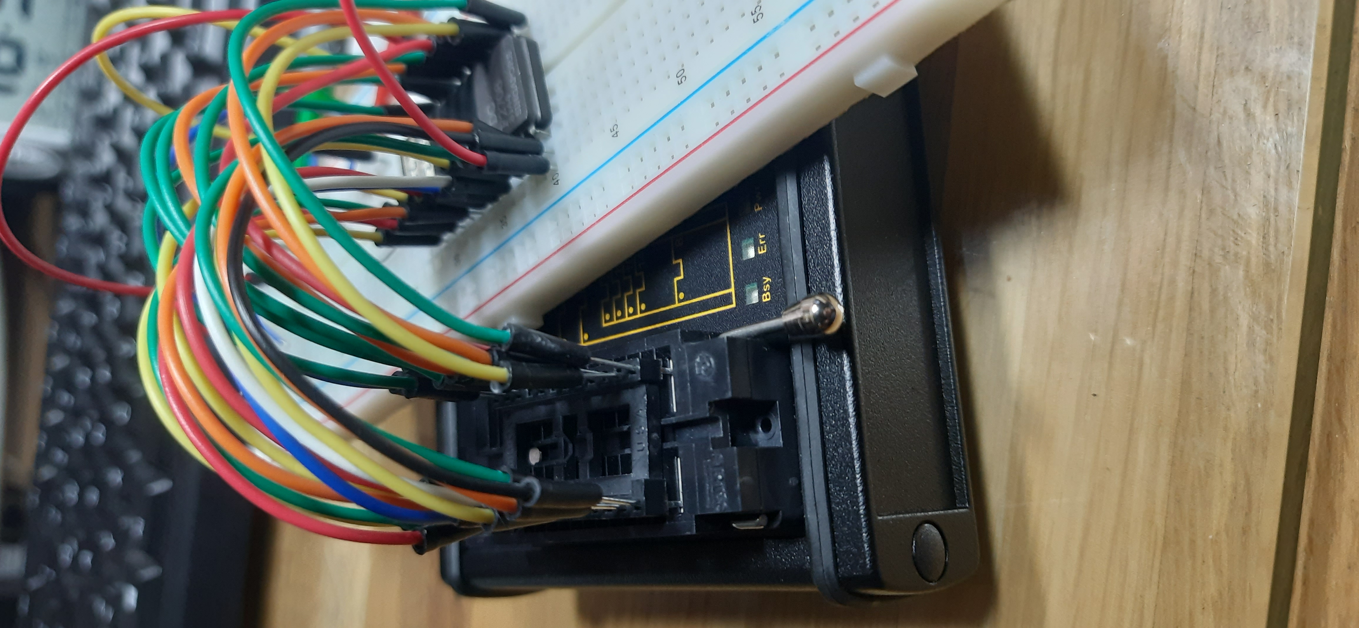
ROM was dumped with Batronix Barlino II, EPROM set to “AM2716B (read only)”, and a special adapter was created on the fly to map the 2708 pins to the AM2716B pins. 2708 needs -5 volts, + 5 volts and +12 volts, and I had to provide -5 volts and +12 volts from an external power supply.
Image shows Batronix Barlino, and on top of it a breadboard with the 2708. All required wires go to a 24 pin IC socket, which is mounted to Eprommers test socket. The two rewuired additional voltages (-5 and +12 volts) are provided from an external power supply.
First analysis:
0x0000-0x03ff    ROM
0x0400-0x04ff    RAM 256 Bytes, Stack starts with highest value in RAM 0x04e

0x0500-0x0506    assumed: access to some hardware
0x0604-0x0614    assumed: access to some hardware
0x0701-0x0706    assumed: access to some hardware
We have the listener HW, talker HW and GPIB. Maybe around 0x0500 is listener, 0x0700 is talker and 0x0600 is GPIB. Why?
- 0x0500 and 0x0700 have about same size
- 0x0600 seems to need more bytes, so could be GPIB
Improved ROM dump: rom-with-labels.txt
Use
Data transfer is done with characters. They are handled in a special way, and different depending on direction.
Data conversation direction “Coupler -> Instrument”
The upper 4 bits of each character D are ignored. Only lower 4 bits are used for sending to J3 connector pins.
- Each character D can be of [0-9,:;<=>?].
- ASCII values for ‘0’-‘9’ are converted to BCD code (4 bits 0000-1001).
- Byte values 1010..1111 are replaced with special characters
In summary, the chars are converted like this:
| D | Hex Code | BCD |
|---|---|---|
| 0 | 0000 | |
| 1 | 0001 | |
| 2 | 0010 | |
| 3 | 0011 | |
| 4 | 0100 | |
| 5 | 0101 | |
| 6 | 0110 | |
| 7 | 0111 | |
| 8 | 1000 | |
| 9 | 1001 | |
| : | 0x3a | 1010 |
| ; | 0x3b | 1011 |
| < | 0x3c | 1100 |
| = | 0x3d | 1101 |
| > | 0x3e | 1110 |
| ? | 0x3f | 1111 |
Data conversation direction “Instrument -> Coupler”
Instrument data comes in 4 bit groups, nibbles.
- Incoming code can be any of 0000-1111
- BCD code (4 bits 0000-1001) are converted to ‘0’-‘9’ ASCII values
- Byte values 1010..1111 are replaced with special characters
Here we can see the nature/origin of the coupler, which expects these nibbles are digits of measurement instruments, looking like “-1.945E06”
| D | ASCII Hex code | ASCII character |
|---|---|---|
| 0000 | 0x30 | 0 |
| 0001 | 0x31 | 1 |
| 0010 | 0x32 | 2 |
| 0011 | 0x33 | 3 |
| 0100 | 0x34 | 4 |
| 0101 | 0x35 | 5 |
| 0110 | 0x36 | 6 |
| 0111 | 0x37 | 7 |
| 1000 | 0x38 | 8 |
| 1001 | 0x39 | 9 |
| 1010 | 0x2b | + |
| 1011 | 0x2d | - |
| 1100 | 0x2e | . (dot) |
| 1101 | 0x2c | , (comma) |
| 1110 | 0x45 | E |
| 1111 | 0x20 | SPACE |
Digit most left:
- Pin 7 = Nibble pin 1, i.e. the x in “000x”.
- Pin 8 = Nibble pin 2, i.e. the x in “00x0”.
- Pin 9 = Nibble pin 3, i.e. the x in “0x00”.
- Pin 10 = Nibble pin 4, i.e. the x in “x000”.
Next digit:
- Pin 11 = Nibble pin 1, i.e. the x in “000x”.
- Pin 12 = Nibble pin 2, i.e. the x in “00x0”.
And so on. I will provide full connector pin drawing later.
Writing to 4883 (4883 as listener)
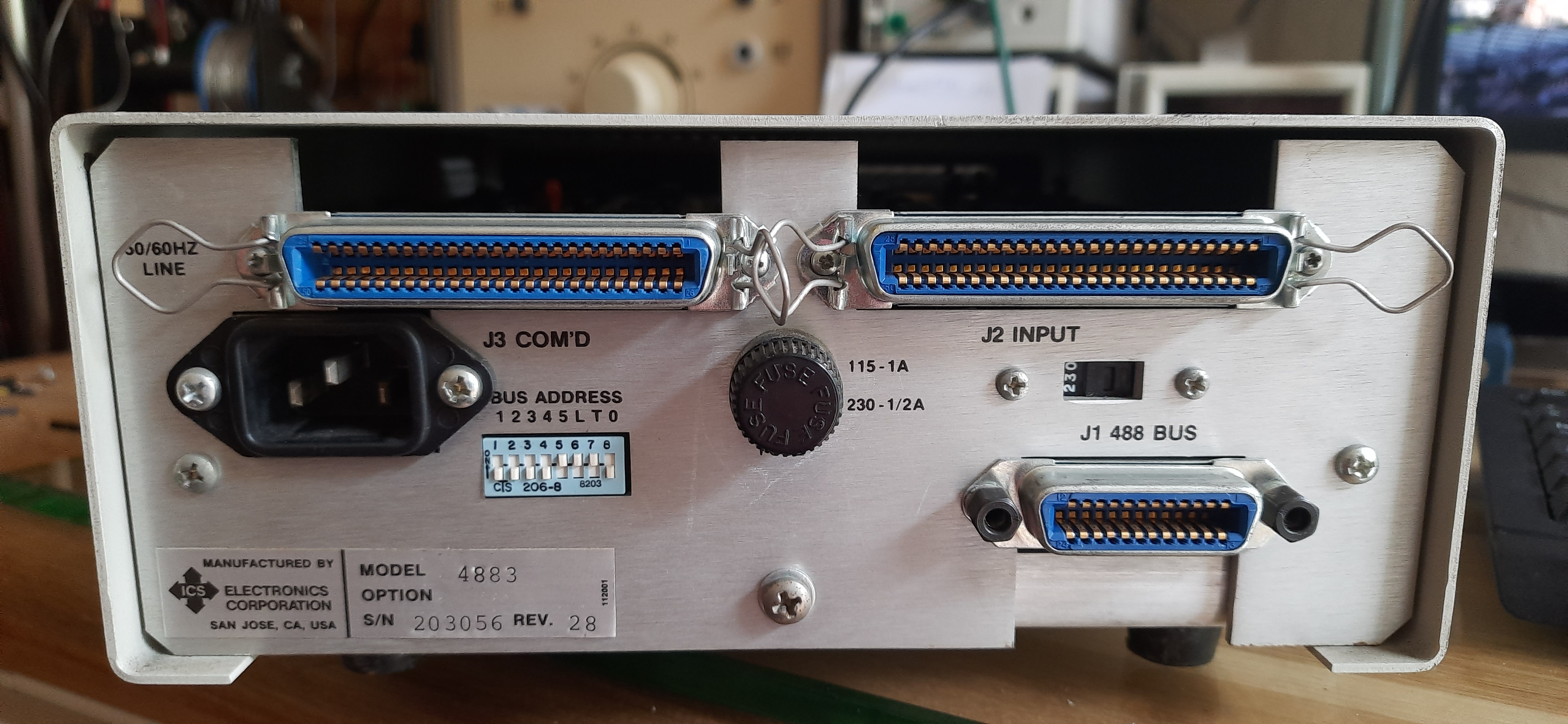
Writing to 4883 means that bits are set/cleared at 50 pin output connector J3 named “Com’D”, according to control data sent via GPIB.
Two pins have +5 volts and GND. From spec, 4883 has 40 output lines. I could see that all 50 pins are connected to the PCB. This means that 50-40-2=8 pins are of yet unknown functionality.
When addressed as listener, we can send a string of content “DDDDDDDDDD\n\r”, i.e. 10 characters and CR,LF.
For 10 character, we can control 10*4=40 output pins.
A write lasts less than 9ms, which is fast for GPIB.
ibtest
Do you wish to open a (d)evice or an interface (b)oard?
        (you probably want to open a device): 16
Do you wish to open a (d)evice or an interface (b)oard?
        (you probably want to open a device): d
enter primary gpib address for device you wish to open [0-30]: 16
trying to open pad = 16 on /dev/gpib0 ...
You can:
        w(a)it for an event
        ...
        send group e(x)ecute trigger (device only)
: w
enter a string to send to your device: >>>>>>>>>>
sending string: >>>>>>>>>>

gpib status is:
ibsta = 0x2100  < END CMPL >
iberr= 0

ibcntl = 11
You can:
        w(a)it for an event
        ...
        send group e(x)ecute trigger (device only)
: w
enter a string to send to your device: 0000000000
sending string: 0000000000

gpib status is:
ibsta = 0x2100  < END CMPL >
iberr= 0

ibcntl = 11
You can:
        w(a)it for an event
        ...
        send group e(x)ecute trigger (device only)
Reading from 4883 (4883 as talker)
Reading from 4883 means that bits at 50 pin input connector J2 named “Input”, according to input data, are read via GPIB.
TBD
Deeper analysis of IO board
I can output data. But there is some handshake for output board, but due to missing manuals and such I do not know the exact pin meanings and how to control the handshake.
Furthermore, input is not working at all. Also because I do not know what to do for “input” data.
So I looked deeper at the IO board.
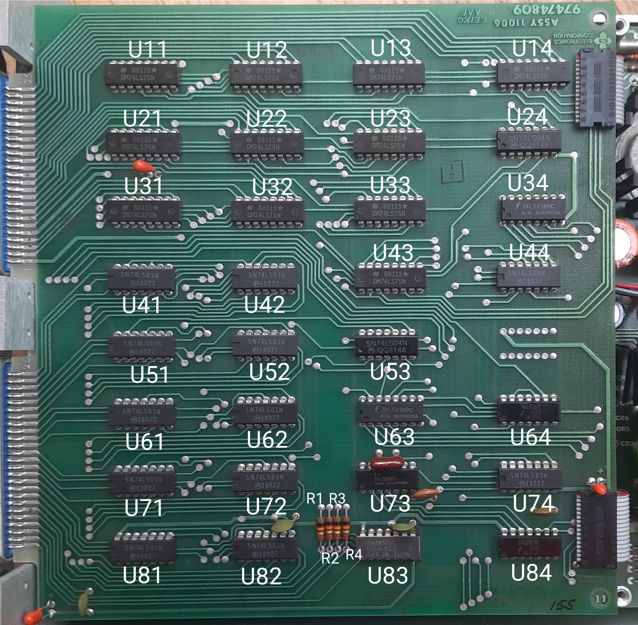
Because there is nothing printed on board, I’ve numbered the chips myself.
Output section
Output handling is done in area of chips U11-U44. (U51-U84 are for input section).
And here is a part of the real schematics, derived from the board.
I’ve only looked at lines from output connector to chips on board. The part from those chips to the controlling connectors was left out.
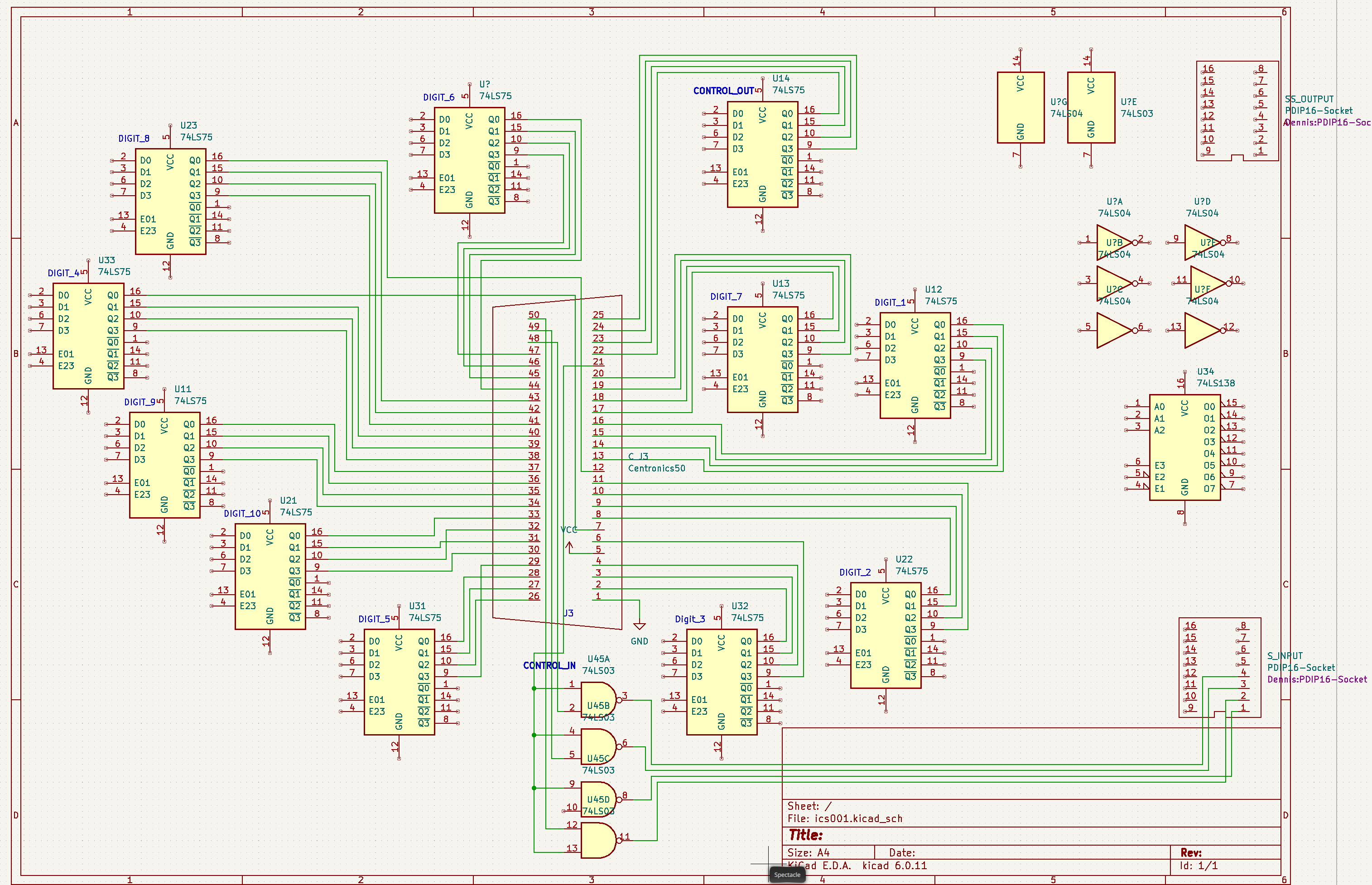
For each output digit, a 4 bit latch is used. We have 10 digits. The chip used is the 74LS75. One additional latch is there, and it is not related to digits! So we have it, a latch with 4 handshake output lines. These are at J3 connector Pin 22-25. Furthermore, there are three input lines, at pins 48-50, also used for handshake.
The input pins just mentioned are enabled by logical HI level at pin 21. If pin21==0, their values will be read by internal logic always as 1, independent of input. if pin21==1, their inverted value will be forwarded to internal logic. Maybe the meaning of this pin is “enable handshake mode” (to be checked).
Finally, we have a ground pin (pin 1) and a Vcc pin with +5 volts (pin 5).
With that information, I can try to find out how handshake is intended to work.
Don’t forget that the aim of communication here is to send a command to an external instrument, and to verify somehow that the command was executed with no issues.
Pins 48-50: I suppose there is a “Device is ready for commands” input, also a “Device command completed”, so at least 2 input lines. Maybe there is an “error condition during command execution”, which would be 3rd input line.
Pin 21: needs to be set to HI in any case, to enable input lines/handshake.
Pin 22-25: The 4 output lines gives more problems. Why so much lines for output control? Maybe we have a “Data available”. But what else? I will try to find out… Maybe among them is a “Device reset” pin, which forwards a GPIB “Universal/Selected Device Clear”.
Table with “special” pins:
| J3 Pin | I/O | Meaning | Comment |
|---|---|---|---|
| 1 | O | GND | |
| 5 | O | +5V | |
| 21 | I | “Enable Handshaking” ? | to be checked |
| 22 | O | ? | |
| 23 | O | ? | |
| 24 | O | ? | |
| 25 | O | ? | |
| 48 | I | ? | |
| 49 | I | ? | |
| 50 | I | ? |
Input section
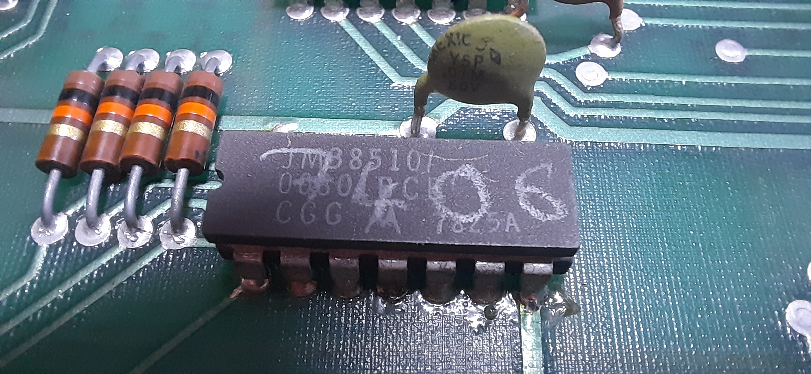
There is one strange chip. Someone has written “7406” with a pencil on it. What is printed on its surface is:
JM38510/
00801 BCB
CGG M 7825A
The M above is Motorola logo. There are numerous ICs with names like “JM38510/…”, it seems these are “Motorola - Military High-Reliability Integrated Circuits”. It also looks like this chip has been replaced as a repair job.
From datasheet examination, this is a 7405 (not a 7406 as written on surface). 7405 has open collector outputs, where 7406 has standard TTL output. The resistors R1-R4 support that this is a 7405 or 74LS05.
Partial schematics:
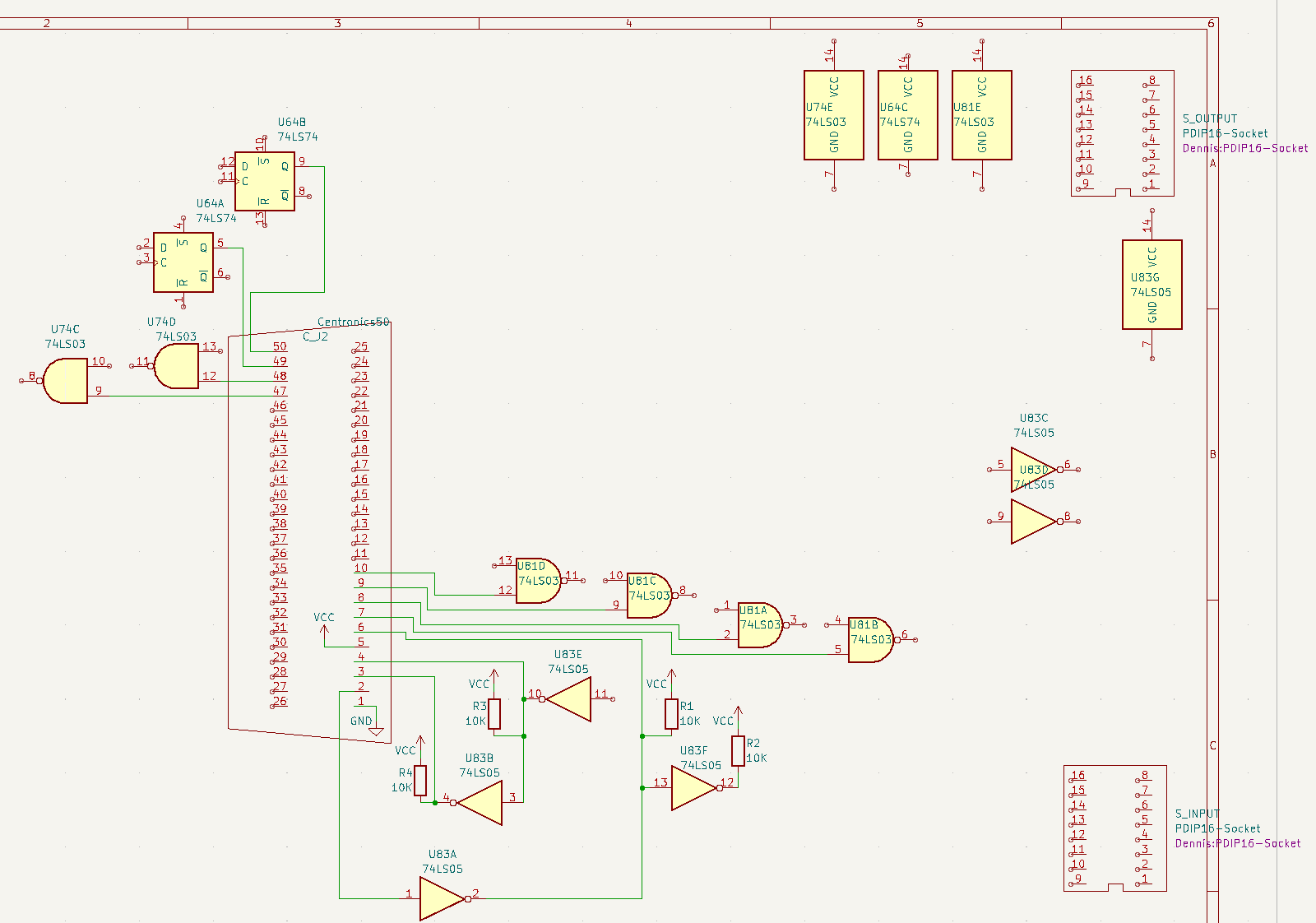
Pin 1 ist GND, pin 5 is Vcc.
Some output control signal comes from internal logic in through inverter U83E.
Its OC output is pulled
up via 10K to Vcc. This signal goes to connector pin 4. The signal goes also
to a second inverter U83B, also pulled up at its output, and this inverted signal
goes to connector pin 3.
This is probably the “start of read cycle” signal.
Via pin 2 (inverted 2 times U83A and U83F) and pin 6 (inverted 1 time U83F) some input handshake signal comes in. Pin 6 input connector is pulled up to Vcc. I suppose this is kind of “data at connector pins is valid” signal.
Pins 49+50 are also outputs, and are connected to U64, which is a 74LS74, D-Flip-Flops triggered by positive edges, having preset and clear.
Pins 47+48, connected to U74, are input pins. Because with pins 7..46, we have already covered to 40 required input pins for input data, I suppose that pins 47+48 are also pins related to handshake.
With ten 74LS03, the 40=10*4 input bits are fetched. These are at pins 7..46. One 4 bit part is shown in schematics (connector pins 6-10).
Table with “special” pins:
| J2 Pin | I/O | Meaning | Comment |
|---|---|---|---|
| 1 | O | GND | |
| 5 | O | +5V | |
| 2 | I | ? | Inverter to pin 6 |
| 3 | O | ? | |
| 4 | O | ? | Inverter to pin 3 |
| 6 | I | ? | |
| 47 | I | ? | |
| 48 | I | ? | |
| 49 | O | ? | |
| 50 | O | ? |
When playing with these lines I’ve got following results:
- All input pins, are in HI state when not connected. Single exception is Pin 6, details on that pin see next point below. HI is around 4.3 volts, LO around 0.3 volts
- Pins 2 and 6 are input and can be the “Instrument Data Ready” pins. Pin 2 triggers the read in of data pins on raising edge. Pin 6 just adds an inverter with its output connected to pins 2. So Pin 6 triggers the read in on falling edge. Issue: changing state of pins 2 and 6 rarely create a SRQ. So maybe these are not the “Instrument Data Ready” pins? SRQ is only created in a special condition
- Pins 3 and 4 are output and are not the “Start Instrument Data Read” pins. Pin 3 just adds an inverter, with input pin connected to pin 4.
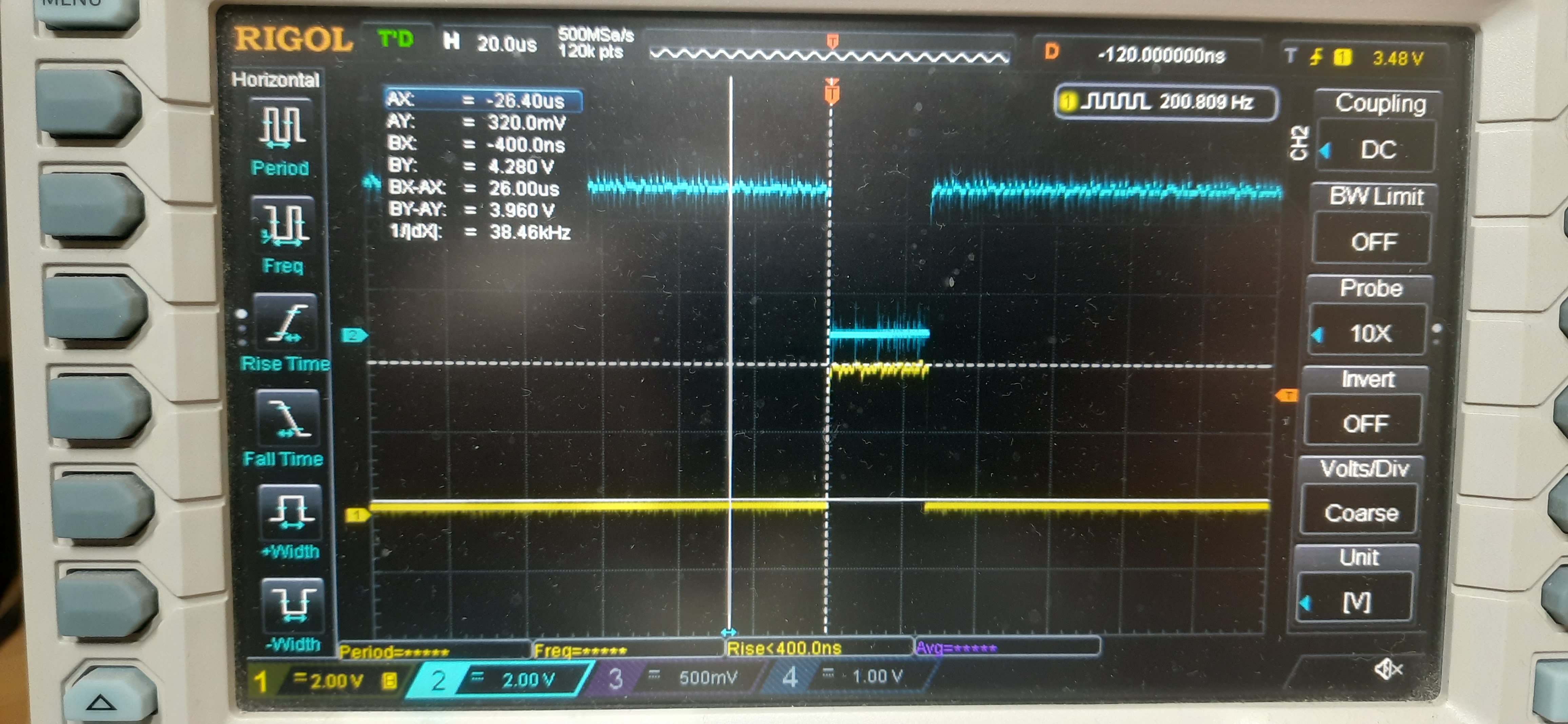
- Pin 50 is the “Start Instrument Data Read”. It gives an LO pulse to start the data read.
Pulse width is ~26µs.
- The pulse is created when sending a device trigger command.
- Pin 49 is signal at Pin 50, but inverted. It gives an HI pulse to start the data read.
- The pulse is created when sending a device trigger command.
Signal at pins 50 (blue) and 49 (yellow):
Fixed table:
| J2 Pin | I/O | Meaning | Comment |
|---|---|---|---|
| 1 | O | GND | |
| 5 | O | +5V | |
| 2 | I | /Instrument Data Ready | Default value = HI. Raising edge triggers 4883 read function. Inverter to pin 6 |
| 6 | I | Instrument Data Ready | Default value = LO. Falling edge triggers 4883 read function |
| 3 | O | /Coupler read data done | Default = HI. Is LO as long as coupler needs stable data at input pins. |
| 4 | O | Coupler read data done | Default = LO. Inverter to pin 3 |
| 47 | I | ? | |
| 48 | I | ? | |
| 49 | O | Start Instrument Data Read | Default = LO. HI pulse triggers Instrument data read. |
| 50 | O | /Start Instrument Data Read | Default = HI. LO pulse triggers Instrument data read. |
Behaviour for SRQ topic (unresolved issue):
- Wenn ich an Pin 2 einen LO HI Übergang erzeuge, gibt es keinen SRQ
- Wenn ich erst “RESET” am Coupler drücke, und dann an Pin 2 einen LO HI Übergang erzeuge, dann gibt es einen SRQ!
Example code in Go
Open device:
import (
    ...
    "github.com/msiegen/linuxgpib"
    "github.com/msiegen/linuxgpib/internal"
)

var opts []linuxgpib.Option
if *verbose {
    opts = append(opts, linuxgpib.Log(log.Default()))
    opts = append(opts, linuxgpib.Timeout(1000*time.Millisecond))
}

d, err := linuxgpib.NewDevice(*board, *address, opts...)
if err != nil {
    fmt.Fprintln(os.Stderr, "Failed to open device:", err)
    os.Exit(1)
}
defer d.Close()
Output data
The following code accesses all 40 output bits. Each pin is written a “1” to, all other pins are “0”.
The loop for all 40 bits:
var num = 0
vmax := 10 * 4

for num < vmax {
    // create output string, like "0080000000"
    queryStr := createCommandString(num)
    if _, err := fmt.Fprintln(d, queryStr); err != nil {
        // ... error handling
    }
    num++
}
Function createCommandString(), which creates a character string, that
defines some bit bumber num to be high, all others low:
func createCommandString(num int) string {
	//queryStr := "0080000000"
	cpos := num / 4
	bpos := num % 4
	queryStr := ""
	var i int
	for i = 0; i < cpos; i++ {
		queryStr += "0"
	}
	queryStr += bitPosToNibble(bpos)
	for j := i + 1; j < 10; j++ {
		queryStr += "0"
	}
	return queryStr
}

func bitPosToNibble(bpos int) string {
	ret := ""
	switch bpos {
	case 0:
		ret = "1"
		break
	case 1:
		ret = "2"
		break
	case 2:
		ret = "4"
		break
	case 3:
		ret = "8"
		break
	}
	return ret
}
Reading from device
We can just try to read data, or use a SRQ for data reading. The first case is working, the SRQ case is still unknown how to do it.
Simple Read
 import (
    ...
	"github.com/msiegen/linuxgpib"
)
Some main loop for the reading:
    var p = []byte{0, 0, 0, 0, 0, 0, 0, 0, 0, 0, 0, 0}
	num := 1
	for true {
		_, _ = d.Read(p)
		pins := prettyPrintPins(p)
		fmt.Printf("%v:\t%v\n", num, pins)

		num++
		time.Sleep(100 * time.Millisecond)
	}
Helper functions:
// prettyPrintPins print bit values
func prettyPrintPins(p []byte) string {
	result := "Read: "
	i := 0
	for i < len(p)-2 {
		bitValue := bitvalue(p[i])
		result += fmt.Sprintf("%v,", bitValue)
		i++
	}
	return result
}

// bitvalue format bit value according to 4883 coupler output data
func bitvalue(b byte) string {
	bvalue := fmt.Sprintf("%x", b)
	switch b {
	case 0x30: 		bvalue = "0000"
	case 0x31:		bvalue = "0001"
	case 0x32:		bvalue = "0010"
	case 0x33:		bvalue = "0011"
	case 0x34:		bvalue = "0100"
	case 0x35:		bvalue = "0101"
	case 0x36:		bvalue = "0110"
	case 0x37:		bvalue = "0111"
	case 0x38:		bvalue = "1000"
	case 0x39:		bvalue = "1001"
	case 0x26:		bvalue = "1010"
	case 0x2d:		bvalue = "1011"
	case 0x2e:		bvalue = "1100"
	case 0x2c:		bvalue = "1101"
	case 0x45:		bvalue = "1110"
	case 0x20:		bvalue = "1111"
	}
	return bvalue
}
Output from program. I have grounded one pin (character 10, bit 3). All other are unused, thus HI level and occur as “1” digits in output.
First three lines are before I’ve created a raising edge on pin 2 (no data).
1:      Read: 0,0,0,0,0,0,0,0,0,0,
2:      Read: 0,0,0,0,0,0,0,0,0,0,
3:      Read: 0,0,0,0,0,0,0,0,0,0,
4:      Read: 1111,1111,1111,1111,1111,1111,1111,1111,1111,0111,
5:      Read: 1111,1111,1111,1111,1111,1111,1111,1111,1111,0111,
6:      Read: 1111,1111,1111,1111,1111,1111,1111,1111,1111,0111,
Read via SRQ
When executing the read() via GPIB call, the coupler generates a pulse on
pin 3/4 of J2, meaning “Start Instrument Data Read”.
I found: When Device Trigger command is send by controller, the coupler generates a pulse on pin 50 of J2, meaning “Start Instrument Data Read”. Nothing happens at pin 3 and 4 (which are also output pins, with unknown meaning so far)
A simple read() does not create a pulse on pin 50 of J2.
After a short while, the external instrument should provide data at the input bits and signal the availability of new data on pin 2 or 6, meaning “Instrument Data Ready”. This should generate a SRQ. (There is a switch at front of coupler “SRQ inhibit”, which will supress SRQ generation)
From SRQ handling, a read() will then return state of all input bits.
As I wrote above, the behaviour is different so far:
Behaviour for SRQ topic:
- Wenn ich Pin 2 mit GND verbinde, gibt es keinen SRQ
- Wenn ich erst “RESET” am Coupler drücke, und dann Pin 2 mit GND verbinde, dann gibt es einen SRQ!
SRQ handling for input data
Check for SRQ and read data:
var p = []byte{0, 0, 0, 0, 0, 0, 0, 0, 0, 0, 0, 0, 0, 0}

for true {
    state, glines := internal.Iblines(*board)
    if err := internal.Err(state); err != nil {
        // some error handling
    }

    // 0x2000 means SRQ occured
    if glines & 0x2000 {
        // Read status byte from device
        sbyte := internal.ReadStatusByte(*board, *address)
        fmt.Printf("Status byte: %x\n", sbyte)
        // 0x41: data available, 0x0 = no data
        if sbyte == 0x41 {
            fmt.Printf("Data available!\n")
            _, _ = d.Read(p)
            fmt.Printf("Read: %x,%x,%x,%x,%x,%x,%x,%x,%x,%x,%x, %x\n",
                p[0], p[1], p[2], p[3], p[4], p[5], p[6], p[7], p[8], p[9], p[10], p[11])
        }
    }
}
References
- Book “PET and the IEE E488 Bus”, with section for ICS Electronics 4883 Instrument Coupler
- Excerpt from book, 4883 pages only
- Fairchild Model 4880 Instrument Coupler Instruction Manual Rev. 5 (1981), Part No. 120002
Used chips:
IO Board:
Main board:
- 2708 EPROM
- 2112 SRAM
- 8080 CPU
- 8080asm.pdf
- Instruction short table - http://dunfield.classiccmp.org/r/8080.txt
- Instruction set - https://popolony2k.com.br/xtras/programming/asm/nemesis-lonestar/8080-z80-instruction-set.html
Some research papers, using 4883:
Mail to ICS
Hello,
I am searching the instruction manual for a very old device that
ICS electronics distributed many years ago. It is the
"ICS Electronics Instrument Coupler 4883", also sold as
"Fairchild Instrument Coupler 4883". There were also versions with
model numbers 4881/4882/4880.

I read somewhere else that it was possible in the past (around 2017)
to get a copy of these manuals for some amount of money + shipping.

Do you offer still this service? I would be very glad.
And one day later a response:
Hello Denni,

Thank you for the inquiry.  I was able to find a copy of an old manual
for the 4880 Instrument Coupler.  We can make a photocopy of it for you.
Price will be $350 which will include Postal Service.

If you are interested, please send me a mailing address and form of
payment will need to be by credit card.  Delivery can take up to 2
to 3 weeks.

Best regards,
(name removed)
Um, no, I am not interested.